Power & energy
Silicon solar cell
Photovoltaics · Semiconductor device
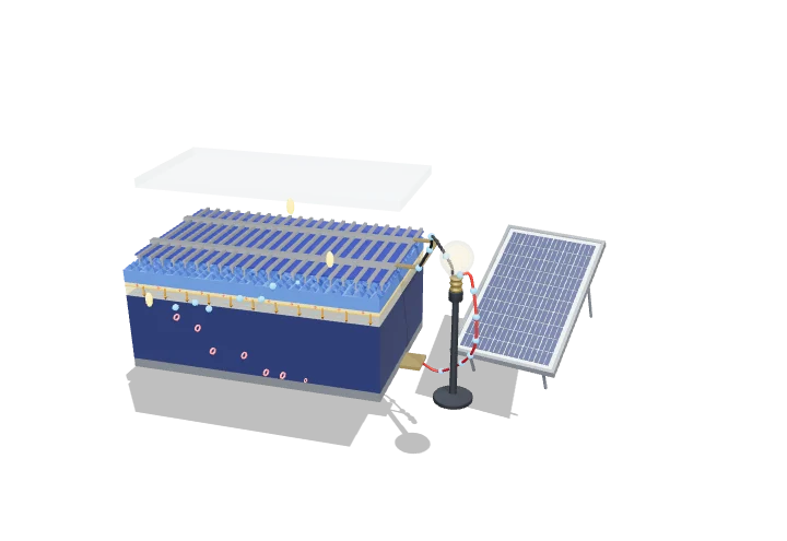 Open the interactive 3D model →
How can a thin slice of sand-derived silicon turn sunlight into electricity with no moving parts?
A solar cell is a thin wafer of silicon made of two layers with slightly different chemistry. When light hits it, it knocks electrons loose, mostly in the thick lower layer, and the boundary between the two layers pushes them one way so they flow out through a wire. Brighter light frees more electrons, so more current flows.
A silicon solar cell is a large-area p–n junction diode: photons with energy above the band gap create electron–hole pairs, and the junction’s built-in field separates them so they flow through an external circuit. Its current is proportional to the light intensity, while its voltage is set by the band gap and recombination, giving commercial efficiencies of about 20–24%.
Key facts
- Silicon band gap
- 1.12 eV at 300 K (absorption edge ≈ 1100 nm)
- Standard test conditions
- 1000 W m⁻², AM1.5G spectrum, 25 °C
- Typical cell (156 mm)
- Isc ≈ 9–10 A, Voc ≈ 0.65–0.72 V, ≈ 4.5–5.5 W
- Efficiency
- ≈ 20–24% commercial; ≈ 27% best laboratory cells
- Wafer thickness
- ≈ 160–180 µm; emitter ≈ 0.3–0.5 µm
- Power temperature coefficient
- ≈ −0.3 to −0.4% per K
Parts you can explore (12)
- Glass cover
- Anti-reflection coating
- Front contacts
- n-type emitter
- Depletion region (p–n junction)
- p-type base
- Back contact
- Photons
- Electrons
- Holes
- External circuit and load
- Solar module
In the 3D model
Rotate and take apart the model, follow a guided tour of what each part does and why it’s needed, change it with a live slider, and test yourself with a short quiz. Free, no sign-up.
Open Silicon solar cell in 3D →
OpenArc Models’ models are simplified teaching schematics. Terms · Privacy