Electromagnetism & electronics
Printed circuit board (4-layer)
Electronics · Manufacturing
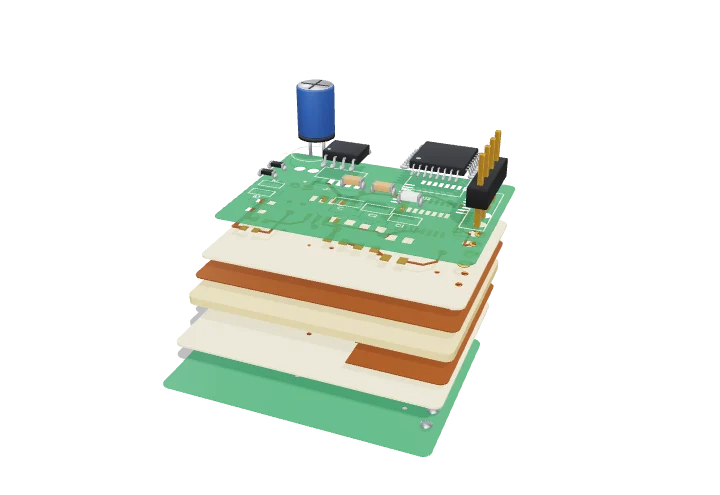 Open the interactive 3D model →
What is hidden inside the thin green board at the heart of every gadget?
A circuit board looks like one flat green card, but it is really a sandwich of thin copper sheets and glass-fibre layers glued together. The copper is etched into “wires” called traces that connect all the chips and parts. Tiny copper-lined holes, called vias, carry connections up and down between the layers.
A printed circuit board is a laminate of insulating glass-epoxy and patterned copper foil that both holds electronic components and wires them together. A four-layer board adds two internal copper planes for ground and power, connected to the outer signal layers by plated vias.
Key facts
- Standard board thickness
- 1.6 mm (0.062 in)
- Copper weight
- 1 oz/ft² ≈ 35 µm thick (outer layers often plated to ≈ 45–50 µm)
- FR-4 permittivity ε_r
- ≈ 4.2–4.7 (frequency-dependent)
- Typical trace / space
- ≈ 0.1–0.25 mm on standard boards; < 50 µm on HDI
- Through-via drill
- ≈ 0.2–0.4 mm; laser microvias ≈ 0.1 mm
- Lead-free solder (SAC305)
- Melts ≈ 217–220 °C
Parts you can explore (13)
- Silkscreen
- Top solder mask
- Top copper (L1)
- Prepreg
- Ground plane (L2)
- FR-4 core
- Power plane (L3)
- Bottom copper (L4)
- Bottom solder mask
- Plated vias
- SMD components
- Solder joints
- Through-hole parts
In the 3D model
Rotate and take apart the model, follow a guided tour of what each part does and why it’s needed, change it with a live slider, and test yourself with a short quiz. Free, no sign-up.
Open Printed circuit board (4-layer) in 3D →
OpenArc Models’ models are simplified teaching schematics. Terms · Privacy