Electromagnetism & electronics
p–n junction diode
Electronics · Semiconductor devices
 Open the interactive 3D model →
How can a tiny chip of silicon let electricity through one way but block it the other?
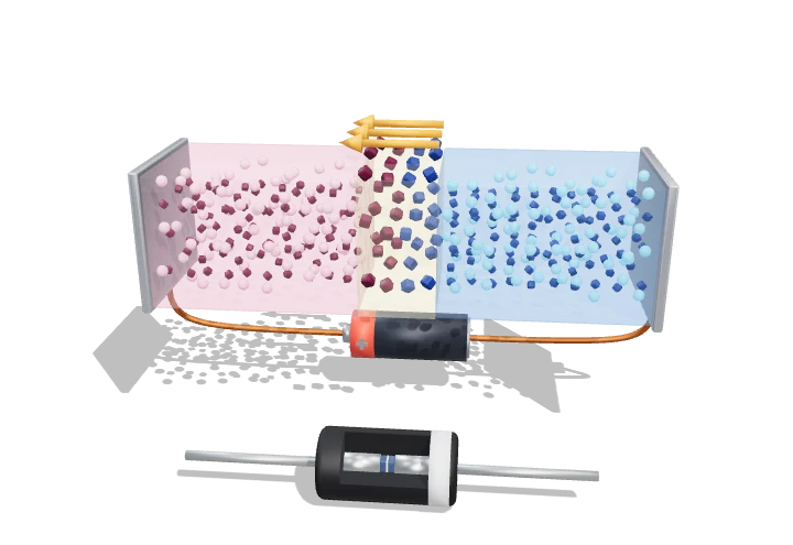
A diode is a piece of silicon treated so that one half has extra free electrons and the other half has “holes” — gaps where electrons are missing. Where the halves meet, the electrons and holes cancel out, leaving a thin barrier zone. Push current one way and the barrier shrinks so current flows; push it the other way and the barrier grows and almost nothing gets through.
A p–n junction forms where p-type and n-type semiconductor meet: carriers diffuse across, leaving a depletion region of fixed ions whose built-in field stops further diffusion. An applied voltage lowers or raises that barrier, so the junction conducts exponentially in one direction and almost not at all in the other.
Key facts
- Silicon band gap
- 1.12 eV at 300 K
- Built-in potential (Si)
- ≈ 0.6–0.9 V, depending on doping
- Depletion width
- ≈ 0.1–1 µm typical; 0.43 µm for N_A = N_D = 10¹⁶ cm⁻³ at 0 V
- Thermal voltage kT/q
- 25.9 mV at 300 K
- Forward drop (Si)
- ≈ 0.6–0.7 V at mA currents; ≈ 1 V at 1 A in a 1N4001
- Current slope (ideal)
- ≈ 60 mV per decade at 300 K (n = 1)
Parts you can explore (12)
- p-type region
- n-type region
- Depletion region
- Acceptor ions
- Donor ions
- Holes
- Free electrons
- Built-in electric field
- Metal contacts
- Bias source
- Injected carriers
- Diode package
In the 3D model
Rotate and take apart the model, follow a guided tour of what each part does and why it’s needed, change it with a live slider, and test yourself with a short quiz. Free, no sign-up.
Open p–n junction diode in 3D →
OpenArc Models’ models are simplified teaching schematics. Terms · Privacy