Electromagnetism & electronics
Integrated circuit: package to transistor
Electronics · Microelectronics
 Open the interactive 3D model →
How do you fit 16 billion switches onto a chip smaller than a postage stamp?
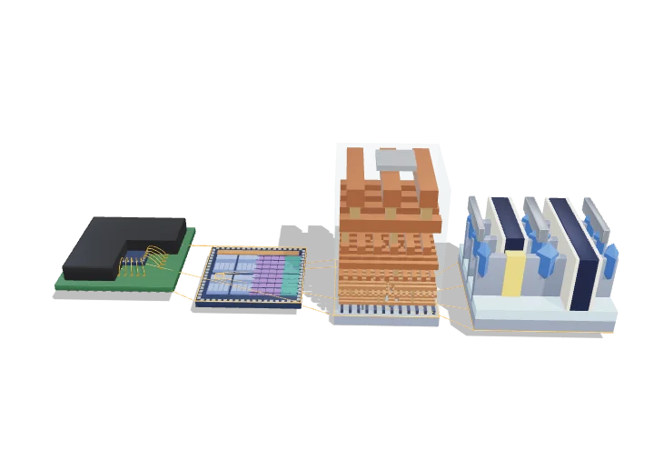
A computer chip is a thin square of silicon covered in billions of tiny switches called transistors, each far smaller than a virus. Above them sits a many-layered city of copper wires that connects the switches together. The whole thing is sealed in a black package with metal balls underneath that join it to the circuit board.
An integrated circuit builds billions of transistors and the wiring between them on one piece of silicon, then seals it in a package that connects it to a circuit board. Zooming from package to transistor spans about six orders of magnitude, from centimetres to a few nanometres.
Key facts
- Transistors on a large processor
- ≈ 10¹⁰–10¹¹ (Apple M1, 2020: 16 billion)
- Typical die area
- ≈ 50–800 mm²
- Copper wiring layers
- ≈ 10–19 in leading-edge logic
- Finest metal pitch
- ≈ 23–40 nm at the 3–7 nm nodes
- FinFET fin width
- ≈ 5–8 nm
- Wafer diameter
- 300 mm (≈ 600 dies of 100 mm²)
Parts you can explore (14)
- BGA substrate
- Solder balls
- Mould cap
- Bond wires
- Silicon die
- Lower metal layers
- Upper metal layers
- Vias
- Contacts and transistor layer
- Dielectric (low-k)
- Silicon fins
- Metal gates
- Source and drain
- Zoom frames
In the 3D model
Rotate and take apart the model, follow a guided tour of what each part does and why it’s needed, change it with a live slider, and test yourself with a short quiz. Free, no sign-up.
Open Integrated circuit: package to transistor in 3D →
OpenArc Models’ models are simplified teaching schematics. Terms · Privacy