Electromagnetism & electronics
Bipolar junction transistor (NPN)
Electronics · Semiconductor devices
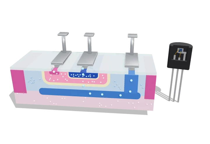 Open the interactive 3D model →
How can a trickle of current control a flow a hundred times bigger?
A transistor is a tiny sandwich of three slices of specially treated silicon: emitter, base and collector. A small current into the thin middle slice, the base, opens the way for a big stream of electrons to rush from the emitter straight through to the collector. That is how a weak signal can switch or boost a much stronger one.
A bipolar junction transistor is two back-to-back p–n junctions sharing a very thin base: the forward-biased emitter junction injects carriers that the reverse-biased collector junction collects. Because the base current needed to sustain this is only about 1% of the collector current, a small current controls a large one.
Key facts
- Structure
- Emitter n+ / base p / collector n (NPN)
- Current gain β (h_FE)
- ≈ 50–300 for small-signal parts; 100–300 for a 2N3904 at 10 mA
- V_BE when conducting
- ≈ 0.6–0.7 V (silicon)
- V_CE(sat)
- ≈ 0.05–0.3 V
- Base width
- ≈ 0.1–1 µm in modern devices
- Transconductance
- g_m = I_C/V_T ≈ 40 mS per mA at 300 K
Parts you can explore (13)
- Emitter (n+)
- Base (p)
- Collector (n)
- n+ buried layer
- Collector sinker (n+)
- Depletion regions
- p-type substrate
- Isolation (p+)
- Field oxide
- Metal contacts
- Injected electrons
- Base current holes
- TO-92 package
In the 3D model
Rotate and take apart the model, follow a guided tour of what each part does and why it’s needed, change it with a live slider, and test yourself with a short quiz. Free, no sign-up.
Open Bipolar junction transistor (NPN) in 3D →
OpenArc Models’ models are simplified teaching schematics. Terms · Privacy